- 您现在的位置:买卖IC网 > Sheet目录1228 > MAX5970EVKIT+ (Maxim Integrated Products)EVAL KIT MAX5970
�� �
�
�0V� to� 16V,� Dual� Hot-Swap� Controller� with� 10-Bit�
�Current� and� Voltage� Monitor� and� 4� LED� Drivers�
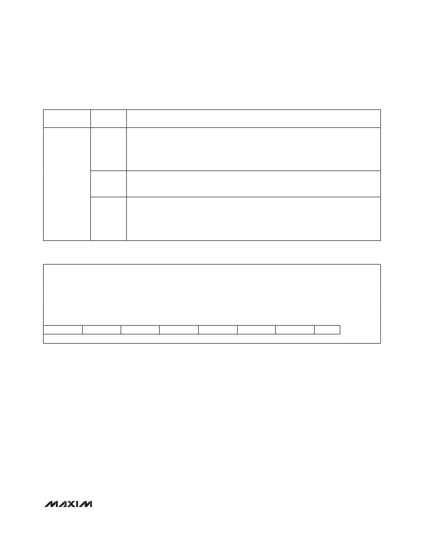
�Table� 4a.� status1� Register� Function�
�REGISTER�
�ADDRESS�
�0x32�
�BIT�
�RANGE�
�[1:0]�
�[4]�
�[7:6]�
�DESCRIPTION�
�ON_� Inputs� State�
�1� =� ON_� above� 600mV� channel� enable� threshold�
�0� =� ON_� below� 600mV� channel� enable� threshold�
�Bit� 0:� ON1�
�Bit� 1:� ON2�
�Channel� Grouping� Mode� (MODE� Input)�
�0� =� Grouped� (MODE� high� or� open)�
�1� =� Independent� (MODE� low)�
�Voltage� Critical� Behavior� (PROT� Input)�
�00� =� Assert� ALERT� upon� UV/OV� critical� (same� as� UV/OV� warning� behavior)�
�01� =� Assert� ALERT� and� deassert� PG_� upon� UV/OV� critical�
�10� =� Assert� ALERT� ,� deassert� PG_,� and� shutdown� channel(s)� upon� UV/OV� critical�
�11� =� (Not� possible)�
�Table� 4b.� status1� Register� Format�
�Description:�
�Register� Title:�
�Register� Address:�
�Channel� grouping� (three-state� MODE� input),� fault-detection� behavior� (three-state� PROT� input),� and�
�ON_� inputs� status� register�
�status1�
�0x32�
�R�
�prot[1]�
�bit� 7�
�R�
�prot[0]�
�bit� 6�
�R�
�—�
�bit� 5�
�R�
�mode[0]�
�bit� 4�
�R�
�—�
�bit� 3�
�R�
�—�
�bit� 2�
�R�
�ON2�
�bit� 1�
�R�
�ON1�
�bit� 0�
�RESET�
�VALUE�
�0x00�
�Figure� 1� shows� the� detailed� logic� operation� of� the� hot-�
�swap� enable� signals� Chx_EN1,� Chx_EN2,� and� ON_,� as�
�well� as� the� effect� of� various� fault� conditions.�
�An� input� undervoltage� threshold� control� for� enabling�
�the� hot-swap� channel� can� be� implemented� by� placing�
�a� resistive� divider� between� the� drain� of� the� hot-swap�
�MOSFET� and� ground,� with� the� midpoint� connected� to�
�ON_.� The� turn-on� threshold� voltage� for� the� channel� is�
�then:�
�V� EN� =� 0.6V� x� (R1� +� R2)/R2�
�The� maximum� rating� for� the� ON_� is� 6V;� do� not� exceed�
�this� value.�
�Startup�
�When� all� conditions� for� channel� turn-on� are� met,� the�
�external� n-channel� MOSFET� switch� is� fully� enhanced�
�with� a� typical� gate-to-source� voltage� of� 5V� to� ensure�
�a� low� drain-to-source� resistance.� The� charge� pump� at�
�each� GATE_� driver� sources� 5� F� A� to� control� the� output�
�voltage� turn-on� voltage� slew� rate.� An� external� capacitor�
�can� be� added� from� GATE_� to� GND_� to� further� reduce� the�
�voltage� slew� rate.� Placing� a� 1k� I� resistor� in� series� with�
�this� capacitance� prevents� the� added� capacitance� from�
�increasing� the� gate� turn-off� time.� Total� inrush� current� is�
�the� load� current� summed� with� the� product� of� the� gate�
�voltage� slew� rate� dV/dt� and� the� load� capacitance.�
�______________________________________________________________________________________�
�15�
�发布紧急采购,3分钟左右您将得到回复。
相关PDF资料
MAX5976BEVKIT+
EVAL KIT MAX5976B
MAX5977AEVKIT#
EVAL KIT MAX5977A
MAX5980EVKIT#
EVAL KIT MAX5980
MAX5982CEVKIT#
EVAL KIT MAX5982C
MAX6397SATA+T
IC SW OVERVOLT PROT 8-TDFN
MAX6496EVKIT+
KIT EVAL FOR MAX6496
MAX6651EVKIT
EVAL KIT FOR MAX6651
MAX7325EVKIT+
KIT EVAL FOR MAX7325
相关代理商/技术参数
MAX5971AETI+
功能描述:热插拔功率分布 IEEE 802.3af/at PSE Controller RoHS:否 制造商:Texas Instruments 产品:Controllers & Switches 电流限制: 电源电压-最大:7 V 电源电压-最小:- 0.3 V 工作温度范围: 功率耗散: 安装风格:SMD/SMT 封装 / 箱体:MSOP-8 封装:Tube
MAX5971AETI+T
功能描述:热插拔功率分布 IEEE 802.3af/at PSE Controller RoHS:否 制造商:Texas Instruments 产品:Controllers & Switches 电流限制: 电源电压-最大:7 V 电源电压-最小:- 0.3 V 工作温度范围: 功率耗散: 安装风格:SMD/SMT 封装 / 箱体:MSOP-8 封装:Tube
MAX5971AETI+W
制造商:Maxim Integrated Products 功能描述:IEEE802.3 AT PSE SWITCH - Rail/Tube
MAX5971AEVKIT
功能描述:电源管理IC开发工具 RoHS:否 制造商:Maxim Integrated 产品:Evaluation Kits 类型:Battery Management 工具用于评估:MAX17710GB 输入电压: 输出电压:1.8 V
MAX5971AEVKIT+
制造商:Maxim Integrated Products 功能描述:PD INTERFACE CONTROLLER - Boxed Product (Development Kits)
MAX5971BETI
制造商:Maxim Integrated Products 功能描述:
MAX5971BETI+
功能描述:热插拔功率分布 IEEE 802.3af/at PSE Controller RoHS:否 制造商:Texas Instruments 产品:Controllers & Switches 电流限制: 电源电压-最大:7 V 电源电压-最小:- 0.3 V 工作温度范围: 功率耗散: 安装风格:SMD/SMT 封装 / 箱体:MSOP-8 封装:Tube
MAX5971BETI+T
功能描述:热插拔功率分布 IEEE 802.3af/at PSE Controller RoHS:否 制造商:Texas Instruments 产品:Controllers & Switches 电流限制: 电源电压-最大:7 V 电源电压-最小:- 0.3 V 工作温度范围: 功率耗散: 安装风格:SMD/SMT 封装 / 箱体:MSOP-8 封装:Tube